

| |
 Description
This applet shows the structure of a PLA or
programmable logic array.
Description
This applet shows the structure of a PLA or
programmable logic array.
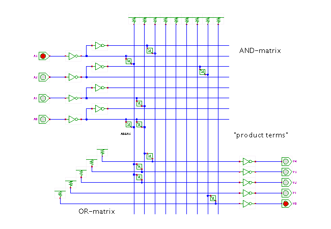
Logically, a PLA is a circuit that allows implementing Boolean functions in sum-of-product form. The typical implementation consists of input buffers for all inputs, the programmable AND-matrix followed by the programmable OR-matrix, and output buffers.
As shown in the applet, the input buffers provide both the original and the inverted values of each PLA input (here called A0, A1, A2, A3). The input lines run horizontally into the AND matrix, while the so-called product-term lines run vertically. Therefore, the size of the AND matrix is twice the number of inputs times the number of product-terms. A weak pullup-resitors ensures that the default value of all product-term signals is high.
Each place in the AND-matrix holds a small diode. Depending on the programming data, this diode is left unconnected, or connected to its input-line and product-line. While the unconnected diode will do nothing, the product-term line will be driven low by the connected diode whenever the corresponding input-line is low. This is the wired-AND operation: a product term will only remain high when none of the (connected!) input-lines is driven low. For example, the leftmost product-line (vertical) in the applet is connected via diodes to both A0 and inverted A3. Therefore, P0 = (!A3 & A0). A similar argument shows that the second product-line P1 = (A2 & A0).
The same structure is repeated in the output (OR-) matrix: the output-lines are driven by weak-pullup resistors, but can be driven low by product-term lines, whenever the corresponding diode is connected during programming.
For example, the upper output line Y4 is connected to both the first (leftmost) and second product-term lines, so that Y4 = P0 | P1, or Y4 = (!A3&A0) | (A2&A0). Similarly, Y0 = P6 | P7 | P8 = A2 | A1 | A0. The remaining product terms and outputs are unused, so that Y3 = Y2 = Y1 = 0.
The main advantage of the PLA structure is that a very compact and space-efficient realization is possible in NMOS technology. Small self-conducting (enhancement-mode) NMOS transistors are used for the pullup-resistors, while a depletion-mode NMOS transistor is placed at each location in the AND- and OR-matrices. The first-level metal mask decides whether to connect the transistors or not. The total-size of a PLA (excluding buffers) is calculated from twice the number of input lines plus the number of output terms times the number of product terms. For many functions, PLAs are much more compact that the discrete realization based on traditional gates. However, the pullup-transistors imply that a PLA draws a (rather large) static current. As low-power consumption is a primary concern in many current devices, PLAs are not as popular in current (CMOS-) technology integrated circuits as they were in the early era of VLSI.
Run the applet | Run the editor (via Webstart)