

| |
 DescriptionThis applet demonstrates how to use
multiple SRAM chips on a single bus
to enlarge memory capacity.
To keep the applet simple, only two memory chips are connected to the bus,
but the same principle can also be used for three and more chips.
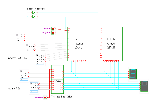
DescriptionThis applet demonstrates how to use
multiple SRAM chips on a single bus
to enlarge memory capacity.
To keep the applet simple, only two memory chips are connected to the bus,
but the same principle can also be used for three and more chips.
Each 6116 SRAM chip holds a a memory matrix of 2048 (2K) words of 8-bit each, addressed by 11 address inputs (A10 .. A0) and accessed via 8 data ports (D7 .. D0). See the previous applet for a demonstration of a single 6116 CMOS SRAM chip.
In a general setup with multiple chips, a so-called address-generator component is responsible to generate the individual chip-selects signals for the different chips connected to the common bus. To avoid short-circuit conditions, at most one component may be enabled to drive the bus at any time. The simplest strategy, called memory-mapping, is to generate the chip-select signals based on the address.
The applet uses only two chips, so that one bit is sufficient to decide which chip to enable. As each chip already uses address bits A10..10, we simply use address line A11 to decide whether to enable the first or the second chip. For addresses in the range 0x000 to 0x7ff the first chip is used, while addresses in the range 0x800 to 0xfff use the second chip. The net result is the same as using a single larger memory chip.
The number of chips connected to one bus is limited by electrical reasons, and usually kept to about a dozen components at most. For example, the memory subsystem of current PC chipsets is usually clocked with about 200 MHz and limited to about two sockets, with up to four memory chips connected to a data-bus line.
To avoid overloading the output transistors of the individual chips, the bus must be split into multiple pieces with additional drivers to connect the parts, if more chips are required. The additional gate-delays through those drivers must be considered for the timing of the bus (e.g. maximum clock frequency). A central arbiter (e.g. the address-decoder) is responsible to enable the drivers that connect the pieces of the bus.
Again, selecting the property editor (popup menu->edit) on the 6116 simulation component opens the user interface with the memory editor. To make more efficient use of screen real estate, eight memory words are shown in each row of the memory. The memory address corresponding to the first memory word of each row is shown on the left, and the remaining words use the following seven memory addresses. Additionally, the memory word last read and written are highlighted in green and cyan colors (unless you use a personalized color scheme). To edit the RAM contents, move the mouse to the memory cell in question, click the left button, and then enter the new value as a hexadecimal number via the keyboard.
The behaviour of the 6116 circuit is controlled by three active-low control lines, namely the chip select and write enable, and output enable inputs: