
| |
 DescriptionThis applets demonstrates the two basic circuits that result
in a dynamic hazards.
DescriptionThis applets demonstrates the two basic circuits that result
in a dynamic hazards.
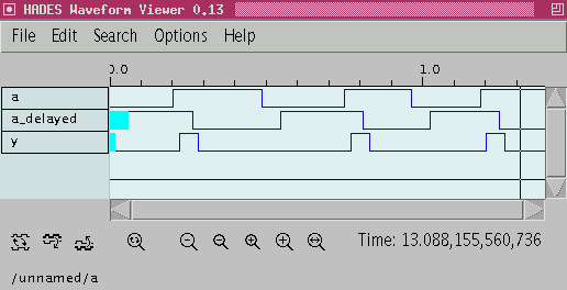
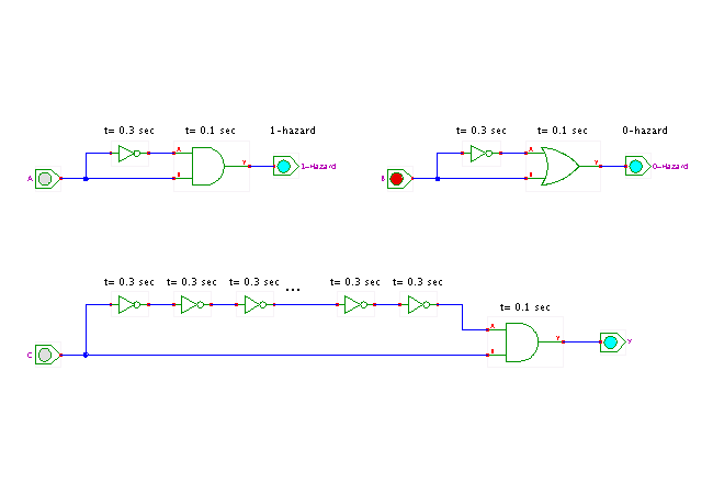
First, the circuit on the top left demonstrates the basic structure responsible for a dynamic 1-hazard (0-1-0 transition). The idea here is to feed the AND gate both with the input value directly, and with a delayed and inverted variant of the input value. Therefore, the stable output value of the circuit is always 0. However, after a rising-edge on the input signal A, the bottom input of the AND gate has the value 1, while the output of the last inverter on the delay-path is also still 1. Therefore, the circuit creates a short 1 pulse after the rising edge of the A input. Again, the actual gate-delays are set to very large values in order to demonstrate the effect in real-time simulation with glow-mode.
Obviously, the second circuit on the top right uses the same basic structure. However, due to the use of an OR gate instead of the AND gate, the default value of the circuit output is 1. A dynamic 0-hazard (1-0-1) is created on the output after each falling edge on the input.The third circuit (bottom) demonstrates the use of gate-delays (and hazards) to generate specific output waveforms, a technique called delay padding. Here, the duration of the 0-1-0 pulse on the output depends on the number of inverters in the delay-line. When using n gates in the delay-line, the output pulse duration is n-times the propagation delay of a single inverter.