TAMS / Java / Hades / applets (print version): contents | previous | nextD-flipflop hazards demo
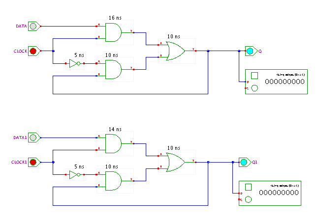
 DescriptionThis circuit demonstrates that hazards have to be considered
very carefully for the design of flipflops and latches.
As the two AND gates together with the OR gate and the inverter
form a 2:1 multiplexer, this circuit is also called a
multiplexer flipflop (or rather, multiplexer latch).
The value on the clock input decides whether the output of the
OR-gate is driven by the data input (when the clock signal is high) or
the delayed feedback output of the flipflop (when the clock is low).
The problem with this type of circuit is its sensitivity to the
propagation-delays of the individual gates.
The initial values (values shown in the frills) in the upper flipflop
are chosen to ensure that the flipflop works.
The main point here is that the delay through the DATA-to-Q path
must be larger than the delay through the feedback-to-Q path.
You may want to play a little with the data and clock inputs to
verify the the flipflop behaves as expected for a standard D-type latch.
However, even a small change in the propagation-delays can introduce
a hazard.
This is demonstrated by the second flipflop, where the DATA-to-Q delay
is slightly smaller than the feedback-to-Q delay.
When both inputs are high, and then the clock changes to low,
a hazard occurs at the OR-gate input.
In the discrete event driven simulation, this results in circuit
oscillations, as the hazard propagates through the feedback path
and results in new events.
In the actual circuit, the flipflop state will depend on the exact
values of all relevant physical quantities (temperature, voltages,
currents, incoming radiation, etc.) and will be undefined.
You can also change the propagation delay of the other gates
and experiment with the circuit.
Run the applet | Run the editor (via Webstart)
Impressum | 24.11.06
http://tams.informatik.uni-hamburg.de/applets/hades/webdemos/12-gatedelay/30-hazards/mux-flipflop_print.html


 DescriptionThis circuit demonstrates that hazards have to be considered
very carefully for the design of flipflops and latches.
As the two AND gates together with the OR gate and the inverter
form a 2:1 multiplexer, this circuit is also called a
multiplexer flipflop (or rather, multiplexer latch).
The value on the clock input decides whether the output of the
OR-gate is driven by the data input (when the clock signal is high) or
the delayed feedback output of the flipflop (when the clock is low).
The problem with this type of circuit is its sensitivity to the
propagation-delays of the individual gates.
The initial values (values shown in the frills) in the upper flipflop
are chosen to ensure that the flipflop works.
The main point here is that the delay through the DATA-to-Q path
must be larger than the delay through the feedback-to-Q path.
You may want to play a little with the data and clock inputs to
verify the the flipflop behaves as expected for a standard D-type latch.
However, even a small change in the propagation-delays can introduce
a hazard.
This is demonstrated by the second flipflop, where the DATA-to-Q delay
is slightly smaller than the feedback-to-Q delay.
When both inputs are high, and then the clock changes to low,
a hazard occurs at the OR-gate input.
In the discrete event driven simulation, this results in circuit
oscillations, as the hazard propagates through the feedback path
and results in new events.
In the actual circuit, the flipflop state will depend on the exact
values of all relevant physical quantities (temperature, voltages,
currents, incoming radiation, etc.) and will be undefined.
You can also change the propagation delay of the other gates
and experiment with the circuit.
Run the applet | Run the editor (via Webstart)