

| |
 DescriptionAn example of using RAM-banks with addition on the i4004 microprocessor
based on this assembly source: ram_add.asm.
DescriptionAn example of using RAM-banks with addition on the i4004 microprocessor
based on this assembly source: ram_add.asm.
; ram_add.asm
; add two BCD numbers on the Intel 4004
init:
       FIM R0R1, 0 ; ram 0, bank 0, address 0
       FIM R2R3, 1 ; ram 0, bank 1, address 0
       FIM R4R5, 2 ; ram 0, bank 2, address 0

       LDM 1
       SRC 0       ; select register 0, address 0
       WRM         ; store 1
       INC R1
       LDM 2
       SRC 0       ; select register 0, address 1
       WRM         ; store 2
       INC R1
       LDM 3
       SRC 0       ; select register 0, address 2
       WRM         ; store 3
       WR0         ; store length 3
       LDM 1
       SRC 1       ; select register 1, address 0
       WRM         ; store 1
       INC R3
       LDM 1
       SRC 1       ; select register 1, address 1
       WRM         ; store 1
       INC R3
       LDM 7
       SRC 1       ; select register 1, address 2
       WRM         ; store 7
       INC R3
       LDM 4
       src 1       ; select register 1, address 3
       WRM         ; store 4
       WR0         ; store length 4
begin:
       SRC 1       ; number 2
       RD0         ; read length
       XCH R6
       SRC 0       ; number 1
       RD0         ; read length
       SUB R6
       JCN NC,len2 ; number 2 >= 1
       JUN go
len2:
       SRC 1

go:
       RD0         ; read length
       XCH R6      ; store length
       LDM 0       ; reset addresses
       XCH R1
       LDM 0
       XCH R3

doAdd:
       JMS ldCarry
       SRC 0
       RDM         ; read digit of number 1
       SRC 1
       ADM         ; add digit of number 2
       DAA
       SRC 2
       WRM         ; write digit of result
       TCC         ; store carry
       XCH R7
       LD R6       ; check length
       DAC
       JCN Z, endAdd ; no digits left, ready
       XCH R6
       INC R1      ; next addresses
       INC R3
       INC R5
       JUN doAdd   ; add next digits

endAdd:
       JMS ldCarry
       JCN NC, len ; carry?
       INC R5
       LDM 1
       SRC 2
       WRM         ; store carry in next digit

len:
       LD R5
       IAC
       WR0         ; write lenght of result

done:
       JUN done    ; end

      ldCarry:
       LDM 15      ; restore carry
       ADD R7
       BBL 0       , return
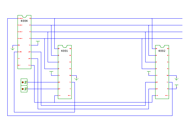
This program demonstrates how the i4004 accesses its data memory, based on the concepts of data-registers. It also shows several basic instructions (e.g. load immediate), subroutines, jumps, etc.
The program starts with the init: part,
which writes some data into the i4002 RAM chip.
The first three FIM instructions initialize register pairs
R0R1, R2R3, and R4R5.
These are later used to address the register-banks 0,1,2
inside the RAM chip.
The LDM instruction (load immediate) next loads the value 1 into the accumulator. The next two instructions, SRC 0 (set register control) and WRM (write memory) write the contents of the accumulator into the selected RAM register cell, which is cell zero in register-bank 0.
To watch the program execution, open the user-interface of the i4004 processor, the i4001 ROM chip memory editor, and the i4002 RAM chip memory editor. (On Windows, you may have to resize and move the windows a little, so that all windows remain readable during the simulation.)
While this program is already a bit longer than the previous programs,
you may still want to single-step through the program
with the technique explained in the MCS4 overview.
Type the value 1.35 into the time-interval textfield
in the simulator control panel,
and select the us (microseconds) value from
the time-scale drop-down list.
Reset the simulation by clicking the rewind button.
Now, click the run-for button to run and automatically
pause the simulation after the selected time interval
(here 1.35 microseconds or one MCS4 clock cycle) has elapsed.
Repeatedly click the run-for button to step through the program.
You might also use a value of 8 cycles (10.8 microseconds)
to run the simulation for one full instruction-cycle instead of
single clock-cycles.
See also:
Run the applet | Run the editor (via Webstart)