

| |
 Description
The applets in this chapter demonstrate the Intel MCS4 system ("Microcomputer System 4-bit"), the first single-chip microprocessor system in history. Despite the complicated memory architecture with separate program- and data-memories, and despite the somewhat incomplete instruction set, the processor and system architecture provide a very interesting engineering solution. Combined with innovative marketing and a complete set of development tools, including an EPROM-based propotype system, the MCS4 became an instant commercial success. While the MCS4 was soon replaced by much better 8-bit systems, it still paved the way for the microprocessor revolution.
The applet above runs a simple endless loop that drives a few LEDs. For a description of this particular MCS4 circuit and program, please click here.
Given the historical interest, the original MCS4 chips and systems are pretty rare and collector's prices are paid for them. Unfortunately, this also holds for the original documentation. For an introduction to the original Intel MCS4 microcomputer system, including scans of the original MCS4 datasheets, visit the Intel 4004 webpages by Paul Pierce. Recently, the Intel museum added a lot of information about the i4004 processor to their website. This includes an overview, the original datasheets (for non-commercial use), and even some images of the original lithography masks. Or read the Wikipedia article on the i4004 system for an overview and a few photos, and visit the CPU Museum i4004 page or Unofficial 4004 web site for photos of the several chips and the Busicom desktop calculator based on the MCS4 system.
A fine overview paper about the MCS4 written by the original developers
appeared in IEEE Micro magazine
to celebrate the 25th birthday of the microprocessor:
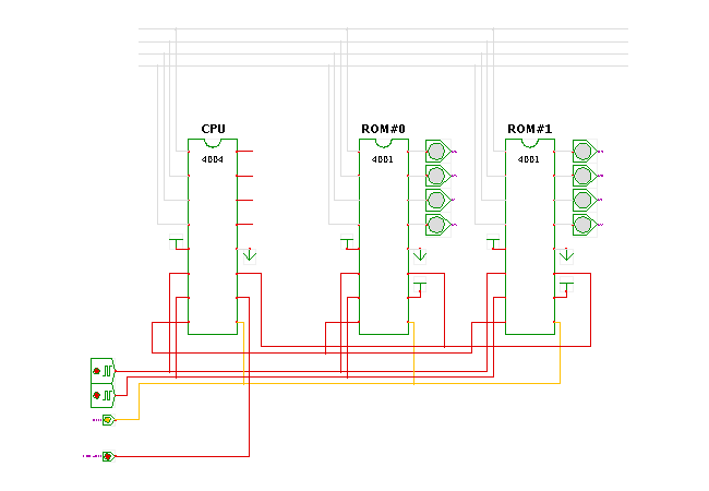
The original chipset as launched in 1971/1972 consisted of three LSI pMOS chips with a common bus-interface, and one additional simpler pMOS chip used to enlarge the I/O capacity:
A minimal MCS4 system consists of one i4004 CPU and one i4001 ROM chip (and a few external components like the two-phase clock generator), while the largest system includes sixteen ROM chips (4 KBytes) and sixteen 4002 RAM chips (640 Bytes).
Later additions to the MCS4 microcomputer system included the i4008/i4009 chipset as an interface to standard (8-bit) memory-chips, and the i4040 microprocessor. Introduced in 1974, the i4040 was faster than the i4004 and added several new instructions including boolean-operations, as well as interrupts.
Probably due to both cost considerations and limitations of the integrated circuit packaging technology of the time, the original chips used standard 16-pin DIL packages - a ceramic carrier for the i4004, and standard plastic packages for the other chips. With two pins for ground and the -15 volts supply voltage, a reset input, and another two clocks signals, only 11 pins remained available for the whole system-bus and the input/output ports on each circuit.
Not surprisingly, the MCS4 system uses an elaborate protocol where both addresses and data are multiplexed onto a single four-bit bus, under control of the i4004 processor. Eight clock cycles are required to process a single instruction, where the last cycle of a instruction is indicated by the SYNC output pin of the i4004 driven low. Given the minimum clock period of 1.35 microseconds (or 740 KHz clock frequency), the original i4004 processor could execute a little less than 100.000 instructions per second.
Every instruction cycle consists of the following phases:
A1: CPU sends address bits
(the four least-significant bits A3..A0)
A2: CPU sends address bits
(the four middle bits A7..A4)
A3: CPU sends address bits
(the four most-significant bits A11..A8)
M1: ROM chip sends instruction bits (D7..D4)
M2: ROM chip sends instruction bits (D3.D0)
X1: CPU executes the instruction.
X2: CPU executes instruction, or I/O data-transfer.
X3: CPU executes instruction,
and the CPU drives the SYNC-output low.
To enable one of the (up to sixteen) ROM and RAM chips, separate chip-select signals are driven by the CPU during the different cycles (together with a few mask-programmed bits in the ROM and RAM chips themselves).
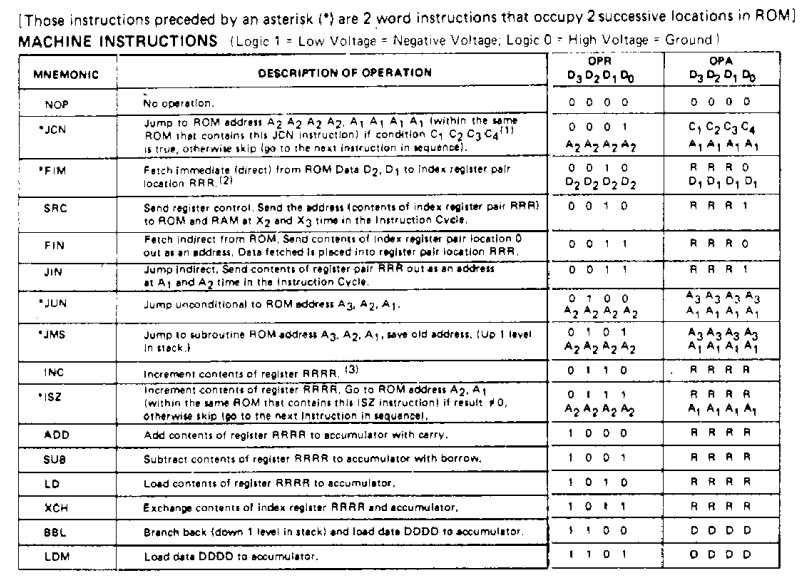
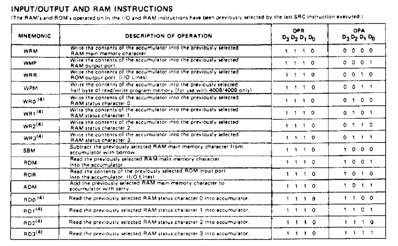
The MCS4 instruction set consists of a total of 46 different instructions, including binary and BCD arithmetic, subroutine calls, data memory transfers, and I/O data transfers. Several instructions are realized as two-word instructions, which execute in two instruction cycles (or 16 clock cycles).
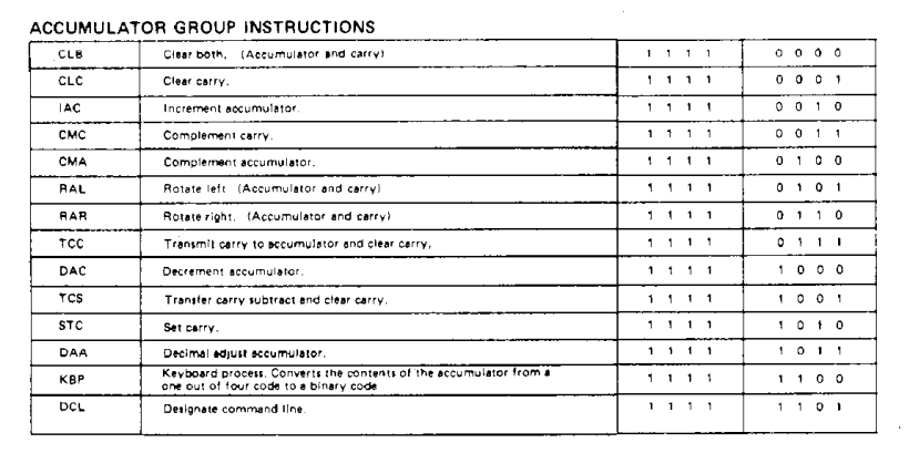
Please consult the above documentation for a full description of the instruction set. Click the following links for three (low-quality) scans: control instructions | RAM and I/O instructions) | accumulator instructions.
Unfortunately, the Intel datasheets fail to specify a few crucial details, such as the exact bit-ordering during address transfers or the internals of a few instructions. As we had no actual hardware for testing and measurements, design choices had to be made in such cases. Still, the simulation models should be accurate on instruction level and assembly-code level, and the simulation models should be able to execute original MCS4 programs. Please let us know if the simulation models behave different than they should.
The user interface of the i4001 ROM and i4002 RAM chip is based on the memory editors used for the other Hades memory components. In the Hades editor, select the 'edit component' menu item from the popup-menu to bring up the memory editor window. Just type in a new (hex) value into the memory editor window to change the corresponding memory contents. Again, the memory cells last read or written are highlighted in green and magenta color. This allows you to watch memory accesses and access patterns easily while the simulation is running. The i4001 memory editor can also show the memory contents in disassembled format, selected via the Edit->Format->Disassemble menu item.
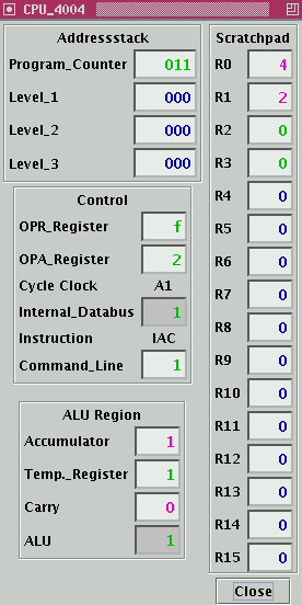
The user interface of the i4004 CPU chip shows the internal registers of the microprocessor. The first panel on the upper left includes the program counter and the three levels of on-chip subroutine stack, where unused entries are initialized to address 0x000. The middle panel on the left side includes several temp registers and also indicates the current instruction cycle (A1,...X3). The bottom panel displays the current values of the accumulator, temp, and carry registers, as well as the current ALU output. The right column shows the current values of the sixteen on-chip scratchpad registers R0, ..., R15. As usual, you can directly edit the textfields to change the corresponding register contents. Please note that the registers are only read during certain bus-cycles, and that changing the control registers within an instruction-cycle may have side-effects.
Warning: the i4004 processor model uses a private variable, called cycleLength, to generate the timing of its output signals. There is currently no user-interface control to read or set the value of this variable, whose default value is 1.35E-6 seconds (the minimum period supported by the i4004), but the value is read and written to the Hades design file. You may have to edit a Hades source file with a normal text editor if you plan to use a clock-period different from 1.35E-6 seconds in your own design files.
The image below shows a screenshot of the i4004 user-interface:
To better watch the execution of our MCS4 demos, you might want to single-step through the programs. After loading a design, just pause the simulation via the pause button in the simulator control panel. Next, enter the value corresponding to one clock-period (single bus-cycle) or eight clock-periods (one instruction) into the text-field right next to the run for button on the simulator control panel. Then, click the run for button to run the simulation for the specified time; depending on the value you typed into the textfield the simulation will execute one clock-cycle, one instruction (single-stepping), or whatever value you have chosen.
For this applet, the clock period is deliberately set to a very large value of 0.02 seconds, so that you can watch the program execution even without single stepping. Therefore, type 0.02 or 0.16 into the textfield and select the 's' (seconds) timescale to execute one clock cycle or one whole instruction cycle, respectively.
In most of the following applets, a clock period of 1.35 microseconds (corresponding to the maximum clock frequency of the original i4004) has been used. Therefore, type the value "1.35E-6" into the simulation control panel textfield at the 's' timescale to single-step those programs.
To run the Hades MCS4 assembler, open a command shell,
include the hades.jar software archive in your CLASSPATH,
and run the hades.models.mcs4.MCS4Assembler program
on your source file. This generates several output files,
including the .rom data files suitable to load into the i4001 ROM chip,
a .hex data file suitable for actual EPROM programming,
and .sym cross reference listing,
and a .lbl file with subroutine labels.
For example:
  rem  use your favorite text editor to write file demo.asm

  cd c:\temp\mcs4
  set CLASSPATH=c:\temp\hades.jar
  java hades.models.mcs4.MCS4Assembler demo.asm
The start the Hades editor, load your MCS4 design into the editor, open the i4001 ROM chip memory editor, and read the newly assembled .rom file (in this example, demo.rom) into the ROM chip. Save your design file, so that the ROM chip stores the .rom filename. Afterwards, you can just re-load the Hades design file to re-initialize your ROM(s) during program development.
Run the applet | Run the editor (via Webstart)