
 |  |
 DescriptionThis applet demonstrates the clock prescaler feature of the
USART 8251 or
universal synchronous and asynchronous receiver and transmitter.
For an overview and register description of the USART chip,
please visit the 8251 overview applet page.
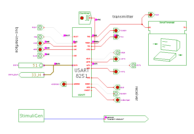
This applet is essential the same as the USART 8251 transmitter demo shown in one of the previous applets. Again, the USART is configured to use eight databits, no parity, and two stopbits, and the serial terminal is setup to those same parameters at 600 baud. The only difference is that the clock-prescaler of the 8251 chip is enabled, at a rate of 16 times. Therefore, the nTXC transmitter bit clock period is now set to 0.104166 milliseconds (1/(600*16)), which again results in a data rate of 600 baud.
The clock prescaler is selected together with the serial communication parameters when writing the mode command to the 8251 chip. The available ratios are 1:64, 1:16, and 1:1 (no prescaler); see the register description in the USART overview page or the original datasheet for details. Using the clock prescaler has two advantages. First, typical quartz oscillators generate frequencies in the megahertz range, while typical baud rates are multiples of 300 baud up to 19200 baud. Having a prescaler on chip means that less external logic is needed to subdivide the quartz oscillator frequencies to the required range. Second, using a prescaler the receiver input signal can be sampled near the middle of the actual bit interval for improved robustness and less sensitivity to differences between transmitter and receiver bit clocks. Once the receiver first detects a startbit, the startbit is confirmed after eight (in 16X mode) or 32 (in 64X modes) input clock cycles, and subsequent data bits are sampled in the middle of the corresponding bit clock interval, also. As this applet only uses the transmitter to demonstrate the prescaler, the sampling of the input signal near the middle of the bit period cannot be seen here. Please run the USART loopback receiver demonstration applet and check that the RXRDY signal is at the middle of the bit period (eight clock after the last bit transition).
The rest of the description is (essentially) the same as the description of the transmitter demo with prescaler.
As you can see, the circuit shown in the applet uses a single 8251 chip, with its TXD data output connected to the RX receiver input of a serial terminal. Therefore, characters transmitted by the 8251 will be decoded and displayed by the terminal, as long as the communication settings of the transmitter and the terminal match. The TXC inputs of the 8251 is driven by a clock generator which is set to a clock period of 0.1041666 mseci - corresponding to 600 baud or 1.6666 msec per bits when considering the 16X prescaler. A stimuli generator component is used to automatically initialize the USART for transmission and to demonstrate the timing of the transmitter and its status signals. The communication parameters of both the 8251 and the terminal are set to eight databits, no parity, and two stopbits.
Once the simulation starts, the stimuli generator component applies the following sequence of input changes to the circuit:
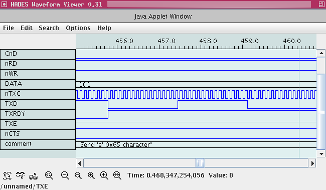
Please check the waveforms to verify that the TXE (transmitter empty) output signal is asserted once the transmitter begins the actual transmission with the startbit. However, the TXRDY (transmitter ready) signal is asserted much later after the second stopbit has been transmitted.
0x0a 0x0d 0x48 0x65 0x6c 0x6c 0x6f 0x2c 0x20 ...
When the automatic sequence has finished, you should take a look at the signal waveforms to check and understand the RS-232 datastream and the values returned by the status register read operations. The waveform of the extra comment signal includes a short description of the ongoing operation. Just click the repaint button in the waveform viewer to update the waveforms, and use the zoom buttons or the zoom-region option to enlarge the areas of interest. For easy comparison between data bus values and transmitter waveforms, you might want to select hexadecimal number format in the waveform viewer (via menu, options, number format, hex). The screenshot below shows the nTXC input clock signal and the TXD data output during a little more than two bit periods in 16X prescaler mode.

To explore the circuit, just continue the simulation via clicking the "run" button (play) in the simulator control panel. You can now use the DATA input switch and the nWR write-enable switch to transmit other data characters via the USART chip. You can also type the following bindkeys to control the applet: 'r' for nRD, 'w' for nWR, 'x' for RESET.
Run the applet | Run the editor (via Webstart)