

| |
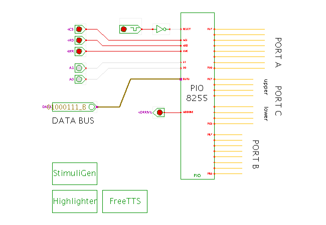 DescriptionThis applet uses a fixed animation sequence to demonstrate
the initialization and some basic input and output operations
using the PIO 8255 or parallel input/output adapter.
The PIO allows connecting a microcomputer system to a variety
of external devices - with very few external components.
DescriptionThis applet uses a fixed animation sequence to demonstrate
the initialization and some basic input and output operations
using the PIO 8255 or parallel input/output adapter.
The PIO allows connecting a microcomputer system to a variety
of external devices - with very few external components.
The whole animation runs for about eight minutes. See the previous applet for the description of the 8255 PIO chip and the fully interactive demonstration. For a typical microprocessor system using the 8255, click here.
  reset  nCS  nRD  nWR  A1  A0  data  |  behaviour
 -------------------------------------+-----------------------------------
      1    *    *    *   *   *     *  |  device reset (mode 0, all inputs)
      0    1    *    *   *   *     *  |  device passive
      0    0    1    1   *   *     *  |  device selected
      0    0    0    1   A1 A0  read  |  read selected register or port
      0    0    1    0   A1 A0  write |  write selected register or port

      u    u    u    u   u   u     *  |  any undefined U,X,Z value will
                                      |  invalidate the simulation model
The chip contains four registers which are selected by two address inputs A1 and A0 during the read and write operations:
  A1 A0
   0  0    port A data register
   0  1    port B data register
   1  0    port C data register
   1  1    control register
The 8-bit data written to the control register configures the 8255 and selects the operation mode, based on the following mapping:
   bit
    D7     1=mode selection 0=single-bit set/reset
    D6D5   groupA mode:  00=mode0 01=mode1 1*=mode2
    D4     portA:        0=output 1=input
    D3     portC-upper:  0=output 1=input
    D2     groupB:       0=mode0  1=mode1
    D1     portB:        0=output 1=input
    D0     portC-lower:  0=output 1=input
The three modes are:
  Mode 0: for basic input and output operations,
  Mode 1: for unidirectional data-transfers with automatic handshake,
  Mode 2: for bidirectional data-transfers with handshake.
Please note that our simulation model only supports mode 0 at the moment. Any attempt to select mode 1 or mode 2 is ignored. Of course, you are welcome to write the additional logic yourself... Please let us know when you do so :-)
For example, writing the data word 0x80 (10000000) into the control register selects mode 0 for all ports and configures all ports as outputs. Afterwards, data written to one of the three data registers will appear immediately on the corresponding pins. On the other hand, writing the data word 0x9b (10011011) into the control register selects mode 0 and configures all ports as inputs. Subsequent read operations of the data registers will return the current input values at the corresponding pins. As a third example, the control word 0x89 (10001001) selects ports A and B as 8-bit outputs, the upper half of port C as a 4-bit output, and the lower half of port C as a 4-bit input. Subsequent writes to the port C data register will now drive the upper four bits of port C, while writing the lower four bits (configured as inputs) is ignored. Similarly, reading the port C data register will return the current four input values of the lower half of port C, merged with the upper four bits from the last port C write operation.
Run the applet | Run the editor (via Webstart)