
 |  |
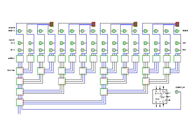
 DescriptionThis circuit demonstrates a slowed-down version
of the modular 16-bit carry-lookahead adder,
so that you can watch how the several carry signals propagate
through the carry-lookahead tree.
Click the input switches or type the '0', .. '9' and 'a' .. 'f' bindkeys to control the values of the B-input switches B0, .., B15 and type the 'x' bindkey to toggle the carry-input. The default values are zero for all A-inputs and ones for all B-inputs. Therefore, changing the carry-input will result in a full carry through all stages of the adder.
As in the previous slowed-down versions of the carry-ripple and carry-select adders, very long gate delays of 0.3 seconds have been preset for each gate. This means that you can easily watch how input changes propagate through the adder-blocks and the carry-lookahead tree. Again, the slowest path is from the least-significant adder block (A0,B0 on the right) to the most-significant adder block (A15,B15). Here, a change of A0 or B0 ripples down through the carry-lookahead tree back to the toplevel carry-lookahead block (bottom left), and then back up to the upper carry-lookahead blocks. This involves two adder-stage delays and 7 stages of the carry-lookahead blocks, while the 16-bit ripple-carry adder obviously involves 16 adder-stage delays. The speed advantage is even greater, because the CLA blocks are simpler and faster than the adder blocks.
The following just repeats the description already presented in the normal-speed version of the applet. The adder consists of 16 1-bit adder blocks and a tree of (8+4+2+1) carry lookahead blocks, which are realized as Hades subdesigns called sum.hds and cla.hds. Both the adder and the CLA are available as separate applets, but you can also just select the "edit" operation in the applet schematics to open the selected subdesign block in a new editor window.
The circuit schematics consists of five rows of related components. The top row consists of 16 LEDs and Hex displays that show the current output value of the adder. Below that are the two rows of 16 input switches for the A (A15..A0) and B (B15..B0) inputs. Below the switches is the row of the adder blocks, each of which connects on its top side to its corresponding Ai and Bi inputs and the Si sum bit. Below the adders is the tree of the carry lookahead generator blocks, whose connections are also illustrated in the bottom right corner. For layout reasons, the carry input switch is also located in the bottom right corner, because it is logically equivalent to the A0 and B0 inputs to the rightmost (least significand) adder. The advantage of the CLA scheme used in this circuit is its simplicity, because each CLA block calculates the generate and propagate signals for two bits only. This is much easier to understand than the more complex variants presented in other textbooks, where combinatorical logic is used to calculate the G and P signals of four or more bits, and the resulting adder structure is slightly faster but also less regular. Exercise: Explain and design the missing logic to calculate the carry-out bit of the adder. Run the applet | Run the editor (via Webstart)