TAMS / Java / Hades / applets (print version): contents | previous | nextD-type latch with NAND gates
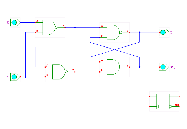
 DescriptionThe D-type latch uses two additional gates in front of the
basic NAND-type RS-flipflop,
and the input lines are usually called C (or clock)
and D (or data).
The function of the D-latch is as follows.
First, note that the clock signal is connected to both of the front NAND gates.
Therefore, if the clock signal is zero, the outputs of the NAND gates
are both 1, and this implies that the RS flipflop stores the previous value.
Therefore, if the C input is 0, the flipflop stores its value.
On the other hand, if the clock signal is 1, the output of the first
NAND gate is the inverse of the D input signal,
and the output of the second nand gate is not(not(D) = D.
This leads to the input values R=0/S=1 or R=1/S=0 on the RS-flipflop,
which in turns enters the corresponding state.
Therefore, if the C input is 1, the flipflop output value follows
to the value on its D input (the latch is 'transparent').
The following timing diagram illustrates this behaviour:
 While the D-latch circuit presented here uses only four two-input NAND gates,
still cheaper implementations are sometimes possible.
For example, a static NAND2 gate in CMOS technology requires four transistors
(two p-type and two n-type each), which results in a total transistor
count of sixteen.
On the other hand, if both the clock signal (C) and the inverted clock
signal are available, it is possible to build a D-latch from two
inverters (two transistors each) and two transmission gates
(two transistors each) with only eight transistors.
If the inverted clock signal is not available, an additional inverter
is required for a total of ten transistors.
For an interactive demonstration of the transmission-gate latch, see our
CMOS
technology demonstration page.
Run the applet | Run the editor (via Webstart)
Impressum | 24.11.06
http://tams.informatik.uni-hamburg.de/applets/hades/webdemos/16-flipflops/20-dlatch/dlatch_print.html


 DescriptionThe D-type latch uses two additional gates in front of the
basic NAND-type RS-flipflop,
and the input lines are usually called C (or clock)
and D (or data).
The function of the D-latch is as follows.
First, note that the clock signal is connected to both of the front NAND gates.
Therefore, if the clock signal is zero, the outputs of the NAND gates
are both 1, and this implies that the RS flipflop stores the previous value.
Therefore, if the C input is 0, the flipflop stores its value.
On the other hand, if the clock signal is 1, the output of the first
NAND gate is the inverse of the D input signal,
and the output of the second nand gate is not(not(D) = D.
This leads to the input values R=0/S=1 or R=1/S=0 on the RS-flipflop,
which in turns enters the corresponding state.
Therefore, if the C input is 1, the flipflop output value follows
to the value on its D input (the latch is 'transparent').
The following timing diagram illustrates this behaviour:
 While the D-latch circuit presented here uses only four two-input NAND gates,
still cheaper implementations are sometimes possible.
For example, a static NAND2 gate in CMOS technology requires four transistors
(two p-type and two n-type each), which results in a total transistor
count of sixteen.
On the other hand, if both the clock signal (C) and the inverted clock
signal are available, it is possible to build a D-latch from two
inverters (two transistors each) and two transmission gates
(two transistors each) with only eight transistors.
If the inverted clock signal is not available, an additional inverter
is required for a total of ten transistors.
For an interactive demonstration of the transmission-gate latch, see our
CMOS
technology demonstration page.
Run the applet | Run the editor (via Webstart)