

| |
 Description
This applet demonstrates the basic inverting tri-state buffer.
Click the input switches or type the 'a' (data-input) and
'e' (enable) bindkeys to control the circuit.
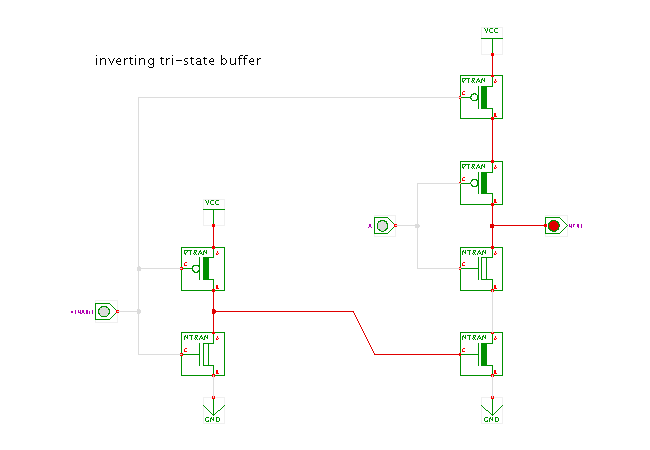
Description
This applet demonstrates the basic inverting tri-state buffer.
Click the input switches or type the 'a' (data-input) and
'e' (enable) bindkeys to control the circuit.
The inverter on the left is required to generate the negated value of the 'enable' input signal. (It can be removed if both the positive and negated value of the 'enable' signal are available from external circuitry.) As shown here, the upper p-channel transistor (driven by the enable input) and the lower n-channel transistor (driven by the inverted enable signal) are conducting whenever the enable input is low. In this case, the inner two transistors are supplied with VCC and GND and behave like a standard inverter. As a result, the tri-state buffer output is the inverted of the data input A.
When the enable input is high, both outer transistor are non-conducting, and the tri-state buffer output is floating ('Z').
  NTRI

  nENA  A  | NTRI
 ----------+------
     1  *  | Z  (floating)
     0  0  | 1
     0  1  | 0
Note that it is possible to exchange the inner and outer transistors without changing the logical function of the gate. (The realization shown here has smaller gate-delay for the A to NTRI path, but reacts slower to changes in the enable signal.)
Run the applet | Run the editor (via Webstart)