
 |  |
 Description
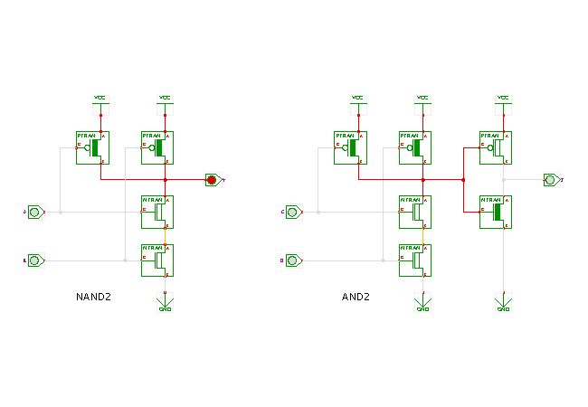
This applet demonstrates the static two-input NAND and AND gates
in CMOS technology.
Click the input switches or type the ('a','b') and ('c','d')
bindkeys to control the two gates.
The two-input NAND2 gate shown on the left is built from four transistors. The series-connection of the two n-channel transistors between GND and the gate-output ensures that the gate-output is only driven low (logical 0) when both gate inputs A or B are high (logical 1). The complementary parallel connection of the two transistors between VCC and gate-output means that the gate-output is driven high (logical 1) when one or both gate inputs are low (logical 0). The net result is the logical NAND function:
  NAND2                  AND2

  A  B  |  Y             A B  |  Z
--------+-----          ------+----
  0  0  |  1             0 0  |  0
  0  1  |  1             0 1  |  0
  1  0  |  1             1 0  |  0
  1  1  |  0             1 1  |  1
As shown on the right, the corresponding AND gate is constructed from the NAND followed by a standard static inverter.
Run the applet | Run the editor (via Webstart)