|
|

|
|
|
|
|
|
Java CMOS Gate Demonstration
|
This page demonstrates how CMOS transistors and basic gates work.
It is intended for our computer science undergraduate students.
The applets were written as a test and working demonstration for
Java/Hotjava.
All comments, hints and bug reports are welcome: Please contact
Norman Hendrich.
Further Java demonstrations on our server (ever wanted to learn
ballroom dancing on the Net?) can be found
here.
|
|
|
Java 1.0 version.
The applets use different colors to indicate voltage levels:
They will only display correctly on a color display.
You need a Java 1.0 (or higher) compatible browser like Netscape, MSIE,
or Suns appletviewer to run the applets.
|
|
Basic CMOS Technology
|
In CMOS (Complementary Metal-Oxide Semiconductor) technology,
both N-type and P-type transistors are used to realize logic
functions.
Today, CMOS technology is the dominant semiconductor technology
for microprocessors, memories and application specific integrated
circuits (ASICs).
The main advantage of CMOS over NMOS and bipolar technology is the much
smaller power dissipation. Unlike NMOS or bipolar circuits,
a CMOS circuit has almost no static power dissipation.
Power is only dissipated in case the circuit actually switches.
This allows to integrate many more CMOS gates on an IC
than in NMOS or bipolar technology, resulting in much better performance.
The following applets demonstrate the N-type and P-type
transistors used in CMOS technology, the basic CMOS inverter,
NAND and NOR gates, and an AOI32 complex gate.
Finally, it demonstrates the CMOS transmission-gate and
a transmisson-gate D-latch.
The first applet illustrates the function of both N-type and P-type
MOS transistors.
Click on the source and gate contacts of the transistors to toggle
the corresponding voltage levels and watch the resulting output
value on the drain contacts.
The applet uses colors to display the different voltages.
- A logical '1' corresponding to electrical level VCC
(typical values for current technolgies are +5V or +3.3V)
is shown in red,
- a logical '0' (corresponding to 0V or GND) in blue.
- A floating wire (not connected to either VCC or GND) is shown in orange.
Note that the N-type transistor is conducting when its input is '1',
while the P-type transistor is conducting when its input is '0'.
The applet displays the channel of a conducting transistor as a
rectangle filled with the color of its source voltage.
The channel of a nonconducting transistor is
shown as rectangle outline in black.
|
|
The CMOS Inverter
|
The most important CMOS gate is the CMOS inverter.
It consists of only two transistors, a pair of one N-type and one P-type
transistor.
The applet demonstrates how the inverter works.
Voltage levels are shown in colors as above: a logical '1' corresponding to
electrical level VCC is shown in red,
a logical '0' (corresponding to 0V or GND) in blue.
Again, a floating wire (not connected to either VCC or GND) is shown in orange.
Because of parasitic effects, the voltage level on such wire may reach
some undefined voltage between VCC and GND after some time.
A floating wire will cause problems, when its voltage is around VCC/2,
because a gate voltage around VCC/2 on either N-type and
P-type transistors implies that the transistor is conducting.
The applet illustrates why this is a serious problem:
When both transistors are conducting, there is a direct path from
VCC to GND, and this implies a short-circuit condition
(shown in light green), which dissipates much energy and may destroy the device.
Click anywhere in the applet to toggle the input voltage for the
inverter from GND to VCC to Z (unknown) to GND.
If the input voltage is '1' (VCC) the P-type transistor on top is
nonconducting, but the N-type transistor is conducting and provides
a path from GND to the output Y. The output level therefore is '0'.
On the other hand, if the input level is '0', the P-type transistor is
conducting and provides a path from VCC to the output Y, so that the
output level is '1', while the N-type transistor is blocked.
If the input is floating, both transistors may be conducting and a
short-circuit condition is possible:
|
|
Power Consumption of the CMOS Inverter
|
The previous discussion of the CMOS inverter shows why CMOS logic
has (almost) no static power dissipation: If the gate voltage is
either '1' or '0' there is no conducting path from VCC to GND,
and there is no static current through the inverter.
In normal operation, the short-circuit condition shown in the applet above
arises only during the very short interval, when the gate voltage
is switched. Typical switching times for the gate are around
1 ns, and the static current dissipation occurs only during a
fraction of this time (while the input voltage is near VCC/2).
All other basic CMOS gates have almost no static power dissipation as well.
But there is a dynamic current dissipation in CMOS gates.
The applet below illustrates this effect for the CMOS inverter.
The gate of a MOS transistor forms a small capacitor. Typical values
for the gate capacity are of order Cg = 10 fF.
If the input of the inverter is connected to VCC at time t1,
this capacitor is charged (Charge Q = Cg * VCC).
If the input is connected to GND at time t2
it is discharged.
The net effect of this is a very small current of
I = dQ/dt = (Cg * VCC)/(t2-t1).
However, due to several reasons the total current drawn by a big
CMOS chip, for example a microprocessor, can be quite large:
- A modern microprocessor may contain about five million transistors,
that is, about one million gates.
Typically, about one percent of all gates switch during one cycle.
- Operating frequencies are up to 200 MHz (cycle time 5 ns)
at an operating voltage of VCC = 3.3V.
- On VLSI chips, the wires connecting the gates have a capacity Cw
that is much bigger than the transistor gate capacities Cg.
When switching an input, not only the transistor gate capacities
but also
the whole wire needs to be charged or discharged: Ctotal=Cg+Cw.
Typical wire loads are about 1 pF
The total current resulting from the short-circuit currents during
switching is difficult to estimate.
But the current resulting from switching the input capacitance alone
is quite large in the example:
I ~ #gates * (Ctotal*VCC) / dt =
(1% * 1.000.000) * (1pF * 3.3V) / 5ns = 6.6 A
On the other hand, the quiescent current in typical static CMOS
ICs is very small. For example, an 2K*8 bit CMOS SRAM dissipates
only 1 uA when idle.
The next applet illustrates the current dissipation in the CMOS inverter.
If the input voltage stays at '1' or '0', either the N-type or the
P-type transistor in nonconducting, and there is no current through
the inverter.
- If the input is switched, the gates of the transistors are
charged/discharged. The applet draws a moving electron to illustrate
this.
- If the input is switched, the input voltage passes the region
near VCC/2, where both transistors are conducting.
That is, during a very short time after each switching, there
is a direct (short-circuit) current through the inverter.
This current again is shown by a moving electron.
The power consumption of static CMOS logic is therefore
directly proportional to switching frequency.
The following plot shows simulated voltages and currents
for a typical inverter. From top to bottom: input voltage,
inverter output voltage, inverter short circuit current,
inverter input current.
|
|
Basic NAND and NOR Gates
|
The following three applets demonstrate the basic 2-input NAND and
NOR gates, and a 3-input NAND gate.
As in all static CMOS gates, each input is connected to the gates
of a pair of N-type and P-type transistor.
Usage of the applets:
The applets are similar to the Inverter applet. Wires with logical '1'
(VCC) are again shown in red, wires with logical '0' (GND) in blue.
Unknown floating values are shown in orange color,
a short-circuit is shown in green.
- Click the mouse near the inputs to toggle the input voltages and
watch the resulting output voltage.
- The corresponding combination of input and output values is
hightlighted in the function-table on the right.
- Click on a function-table entry to select the corresponding input
voltages.
- Clicking on the top line of the function-table will step
through the function-table.
To simplify the applet, only '1' and '0' levels are allowed as input
values. Obviously, a short-circuit may occur in these gates as well,
if the input voltages are floating near VCC/2 (because both N-type and
P-type will be conducting,
thereby providing direct paths from VCC to GND).
|
|
The NOR2 Gate
|
The 2-input NOR gate is the simplest CMOS gate to illustrate the
name complementary MOS:
The P-type transistors are connected in series between VCC
and the output Y, while the N-type transistors are connected in parallel
between GND and the output Y.
That is, the N-type and the P-type parts of the CMOS gate are
complementary (in respect to topology, and therefore function).
Only if both inputs A and B are '0' (corresponding to GND), there
is a conducting path from VCC to the output (output level '1').
A input combination with A or B '1' blocks the path from VCC to the
output, but opens a path from GND to the output (so that the output
level is '0').
Watch the voltage level between the two P-type transistors. If both
are nonconducting, the voltage level is unknown (floating). However,
as that wire is not connected to any MOS-transistor gate,
there is no problem:
|
|
The NAND2 Gate
|
In the two-input NAND gate the P-type transistors are connected
in parallel between VCC and the output Y, while the N-type transistors
are connected in series from GND to the output Y.
|
|
The NAND3 Gate
|
The generalization of the 2-input NOR and NAND gates is obvious.
As an example, the next applet shows a NAND gate with 3-inputs.
As for the 2-input NAND, all (three) P-type transistors are connected
in parallel between VCC and the output Y, while all
N-type transistors are connected in series.
Again, the wires connecting the N-type transistors may have
floating voltage levels when the transistors are nonconducting.
That is no problem, because these wires are not connected to any
transistor gate.
NOR gates with three and more inputs are constructed correspondingly -
all P-type transistors are connected in series and the N-type
transistors are connected in parallel between GND and the output Y.
However, the series connection of transistors implies
longer propagation delay (especially for P-type transistors)
and a voltage drop across the transistors.
Therefore,
NAND gates for actual CMOS cell libraries are usually limited to 4-inputs
(4 N-type transistors in series)
and NOR gates to 3-inputs (3 P-type transistors in series).
NAND and NOR gates with more inputs are realized as a combination
of simpler gates with up to 3 (4) inputs.
|
|
Complex Gates
|
As in NMOS technology, there are certain logic functions that can
be realized very efficiently by CMOS gates.
These gates are called complex gates because they realize
a complex logic function - although the gates themselves are rather
simple.
Typical example for complex gates found in almost all cell libraries
are combinations of AND-OR-INVERT and OR-AND-INVERT gates.
For example, the gate for the logic function Y = !((A ^ B) | (C ^ D ^ E))
- that is, the NOT of the OR of two ANDs - is typically called
an AOI32 gate.
This gate is shown in the next applet. It needs 10 transistors only
(5 pairs of N-type and P-type transistors, one pair for each input).
To simplify the circuit schematic, the input wires are not drawn
completely.
Rather, all input wires are broken into two pieces,
connected to the corresponding N-type and P-type transistors.
For example, to toggle the input voltage for input A, you can click
both near the N-type or the P-type transistor gate connected to input A.
Note that again the N-type and P-type paths in this gate are complementary.
P-type transistors connected in series correspond to N-type transistors
connected in parallel, and vice versa.
The generalization to other complex gates should be obvious.
Again, gates with more than three transistors connected in series
are not used.
Most cell libraries contain gates from AOI21 and OAI21 up to
aOI33 and OAI33.
Try to construct one of these on paper and understand how it works!
|
|
The CMOS Transmission Gate
|
As in NMOS technology, there are certain logic functions that can
be realized very efficiently by CMOS gates.
The first applet on this page demonstrated the switching behaviour of N-type
and P-type transistors.
However, while both N-type and P-type transistors indeed have a very large
resistance between source and drain when switched off, a detailed
analysis reveals that the resistance between source and drain depends
on the source and drain voltages when switched on.
Especially, there is a voltage drop across a conducting N-type transistor when
the source voltage is near VCC, and a voltage drop across a conducting
P-type transistor when its source voltage is near GND.
(Note that thhis poses no problem in the static CMOS gates, where all
source contacts of N-type transistors are connected to GND and all
source contactes of P-type transistors are connected to VCC.)
Therefore, the use of single N-type or P-type transistors as switches
is limited to circuits where the voltage drop across the conducting
transistors is not critical.
A series connection of transistors used as switches is usually not
possible in digital circuits.
But a combination of N-type and P-type transistors allows to realize
efficient switches in CMOS technology. The circuit consists of one
N-type and one P-type transistor connected in parallel and controlled
by inverted gate voltages.
This circuit, called a transmission gate (T-gate)
is demonstrated in the following applet:
- Click on the gate of either the N-type or the P-type transistor
to invert (both) gate voltages.
A T-gate requires that the N-type and P-type transistors have
inverted gate voltages.
- Click on the 'L' (source) or 'R' (drain) contacts to toggle
the corresponding voltage from GND to VCC to Z.
To better demonstrate the switching behaviour of the T-gate,
the new voltage just selected by clicking 'wins' over
the previous value.
If the gate voltage of the N-type transistor is 'GND', the P-type
transistors has a gate voltage of 'VCC' and both transistors are
nonconducting.
On the other hand, if the gate voltage of the N-type transistor is 'VCC'
and the gate voltage of the P-type transistor is 'GND', both transistors
are conducting. If the source voltage is near VCC, there is a voltage
drop across the N-type transistor but (almost) no voltage drop across
the P-type transistor. If the source voltage is near GND, the N-type
transistor has (almost) no voltage drop.
Because of the symmetry of standard MOS transistors, there is no
reason to differantiate between source and drain in a T-gate.
The contacts are therefore usually called 'L' (left) and 'R' (right).
|
|
The CMOS D-Latch
|
In CMOS technology, T-gates allow efficient realizations of several
important logical functions.
Perhaps the most important use is demonstrated in the next applet.
A standard D-latch (level controlled flipflop) can be build from
four 2-input NAND gates. Therefore, 16 transistors are needed
for one D-latch. (Try to construct this circuit on paper - the simple
D-latch circuit is one of our pet examination problems!)
The applets shows how a D-latch can be realized using only
8 transistors (2 inverters and 2 T-gates), if both the clock and
the inverted clock signal are available - a savings of 50% of transistors
and therefore chip-area.
If the inverted clock is not available, an additional
inverter is needed to provide the control signal for the two T-gates,
still with a savings of 10 transistors versus 16.
- Click near the D input to select the data input value for the D-latch.
- Click near the C (clock) or NC (inverted clock) input to toggle
the current clock input value.
To simplify the circuit schematic, the C and NC wires are not
drawn completely. Rather, the corresponding T-gate gate inputs
are labeled with C or NC.
Note that the input T-gate (on the left) is controlled by C,
while the feedback T-gate (on top) is controlled by NC.
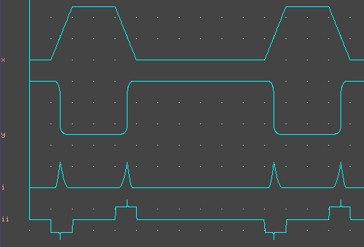
- The current values for data input D, clock input C, and data
output Q are plotted as waveforms on the bottom of the applet.
This allows to demonstrate the data storage in the latch when
the C input is '0'.
- If you click anywhere else, the input voltages are not changed.
However, simulation time is increased, and the waveforms are
updated.
The function of the T-gate D-latch is very easy to understand.
If the C input is '1', the input T-gate is conducting, and the
data input value is connected to the first inverter input, which
generates !D.
The second inverter generates !!D = D, that is, the output Q
equals D (the latch is transparent).
If the C input is switched to '0', the first T-gate is blocked
while the feedback T-gate (whose R contact is connected to Q, which
still equals D) is opened.
Therefore, the circuit feeds its Q signal back to the first inverter
(!Q) and to the second inverter !!Q=Q.
That is, the value of Q is stored until the C input becomes '1' again.
|
|
SRAM cell
|
Please click here for a demonstration of the
six-transistor cell
used for static CMOS memories, e.g. processor cache memories.
|
|
|
|
|
Related topics
on our server
|
|
|
|
http://tams-www.informatik.uni-hamburg.de/applets/cmos/cmosdemo.html |

