
Applets
contents
visual index
 introduction
 std_logic_1164
 gatelevel circuits
 delay models
 flipflops
 adders and arithm...
 counters
 LFSR and selftest
 memories
 ROM circuit
 1Kx8 ROM demo
 RAM structure
 RAM write-cycle
 RAM read-cycle
 RAM write-ha...
 RAM storage ...
 RAM address ...
 RAM bitline ...
 74189 SRAM
 74219 SRAM
 74219 SRAM a...
 6116 CMOS SRAM
 multiple SRAMs
 programmable logic
 state-machine editor
 misc. demos
 I/O and displays
 DCF-77 clock
 relays (switch-le...
 CMOS circuits (sw...
 RTLIB logic
 RTLIB registers
 Prima processor
 D*CORE
 MicroJava
 Pic16 cosimulation
 Mips R3000 cosimu...
 Intel MCS4 (i4004)
 image processing ...
 [Sch04] Codeumsetzer
 [Sch04] Addierer
 [Sch04] Flipflops
 [Sch04] Schaltwerke
 [Sch04] RALU, Min...
 [Fer05] State-Mac...
 [Fer05] PIC16F84/...
 [Fer05] Miscellan...
 [Fer05] Femtojava
 FreeTTS
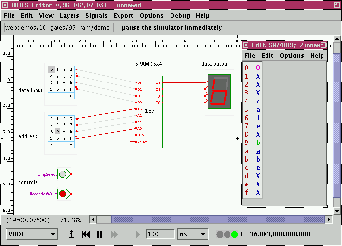
 The behaviour of the 74189 circuit is controlled by just two active-low
control lines, namely the chip select and read/write
inputs:
- nCS=1: the data outputs are tri-stated and the clock signal for the latches in the memory matrix is disabled.
- nCS=0, Read/nWrite=1: the data outputs are enabled and driven with the contents of the currently addressed memory word. When the address input is changed, the contents of the newly selected memory word will appear on the data outputs, delayed by the memory access time.
- nCS=0, Read/nWrite=0: the clock signal of the currently addressed memory latches is enabled, so that the values on the data input bus is copied into the selected memory word (transparent latches). Also, the data outputs are enabled. Switch the Read/nWrite signal back to the high (1) state to store the data.