| CMOS 6116 2Kx8 SRAM
Circuit Description
This applet demonstrates the
CMOS 6116 SRAM circuit.
It consists of a memory matrix of 2048 (2K) words of 8-bit each,
addressed by 11 address inputs (A10 .. A0)
and accessed via 8 bidirectional data pins (D7 .. D0).
Due the the smaller transistor size and the much lower energy dissipation,
CMOS memories can be built with much higher capacity
than bipolar RAMs (like the 74189 demonstrated in the previous applet).
Naturally, current CMOS technologoy allows to manufacture much larger
memories than the 6116 with its 2 KBytes (which was popuplar on the
early 8-bit microcomputers).
Internally, CMOS SRAMs typically employ a standard six-transistor
storage cell that is somewhat smaller than a standard latch and also
allows for very efficient layout (by cell abutment).
Unfortunately, the six-transistor storage cell relies on certain
low-level electrical properties of the transistors that cannot
easily be modelled on the logical level. Therefore, a Hades
simulation model of the storage cell is not included in this applet
collection. Instead, please check out the dedicated
6-transistor
SRAM storage cell demonstration applet on our website.
Unlike the 74189-SRAM shown in the previous applet,
the 6116 integrated circuit uses a single data bus for both
read and write operations.
This is a typical organization for large external memories,
where the number of pins on the circuit package and the number
of signal wires on the boards determine the total system cost.
In fact, typical DRAM circuits with even higher memory capacity
often also use a multiplexed address bus in order to reduce
the number of pins required for the address inputs.
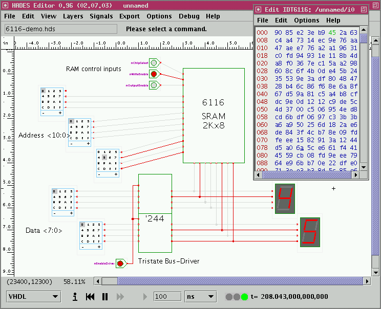
Again, selecting the property editor (popup menu->edit) on the 6116
simulation component opens the user interface with the memory editor.
Eight memory words are shown in each row of the memory.
The memory address corresponding to the first memory word of each row
is shown on the left, and the remaining words use the following seven
memory addresses.
Additionally, the memory word last read and written are highlighted
in green and magenta colors (unless you use a personalized color scheme).
To edit the RAM contents, move the mouse to the memory cell in question,
click the left button, and then enter the new value as a hexadecimal
number via the keyboard.
The 6116 RAM stores 8-bit per memory word,
so that two keystrokes ('0' .. '9', 'a' .. 'f') are required to fill
one data word.
Each new keystrokes adds one hex-digit and shifts-out the previous
memory contents.
Type the space key or shift+space to navigate to the next or previous
memory word.
The following screenshot shows the Hades editor running the 6116
RAM demo with the memory editor open:
 The behaviour of the 6116 circuit is controlled by three active-low
control lines, namely the chip select, write enable,
and output enable inputs:
The behaviour of the 6116 circuit is controlled by three active-low
control lines, namely the chip select, write enable,
and output enable inputs:
- nCS=1: the data outputs are tri-stated and the clock signal
for the latches in the memory matrix is disabled.
- nCS=0, nWriteEnable=1, nOutputEnable=1:
the memory chip is selected but passive.
- nCS=0, nWriteEnable=1, nOutputEnable=0:
the data outputs are enabled and driven with the contents
of the currently addressed memory word.
When the address input is changed, the contents of the
newly selected memory word will appear on the data outputs,
delayed by the memory access time.
- nCS=0, nWriteEnable=0, nOutputEnable=1:
the data outputs are disabled but the write signal for
the internal latches (or rather, 6-transistor storage cells)
is activated. The RAM contents of the currently addressed
memory cell is overwritten with the current input values
on the data bus, which should be driven by external logic.
Switch the nWriteEnable signal back to the high (1) state
to store the data.
- nCS=0, nWriteEnable=0, nOutputEnable=0:
the outputs are enabled, and writing is enabled.
This is not a recommended mode of operation, because
the RAM contents might get overwritten due to hazards.
To get accustomed to the behaviour of the SRAM, it is a good exercise
to try to write a few data words into the memory (e.g. the values
shown in the screenshot above).
Due to the asynchronous interface of the RAM, great care must be
taken to avoid hazard conditions on either of the Read/nWrite and
address inputs.
| | |


 introduction
 memories