

| |
 Description
A switch-level demonstration of the CMOS transmission-gate latch,
shown as a complete transistor-level schematics.
See the next applet for a simplified way to draw this circuit.
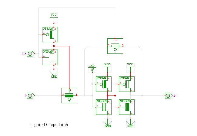
Description
A switch-level demonstration of the CMOS transmission-gate latch,
shown as a complete transistor-level schematics.
See the next applet for a simplified way to draw this circuit.
Click the input switches or type the 'c' and 'd' bindkeys to control the clock and data inputs.
The circuit consists of a t-gate based multiplexer and a non-inverting buffer (built as a cascade of two inverters). One additional inverter (on the top left) is used to generate the inverse of the clock input signal, required to control the transmission-gates. If both the clock signal and the inverted clock signal are available from external circuitry, this inverter can be removed.
The left transmission gate is enabled when the clock input is high, while the right transmission gate is enabled when the clock input is low. Therefore, when the clock input is high, the current value from the data input (D) will propagate through the left transmission gate and through the inverters. The latch is transparent, and the output value Q follows the data input value, while NQ generates the inverse of the data input value.
As soon as the clock signal changes to low (logical 0), the left transmission-gate is switched-off, while the right transmission-gate is activated and becomes conducting. As a result, the output value Q of the flipflop will be fed back into the input of the first-stage inverter. Therefore, the latch stores whatever value it hold when the clock signal changed to low.
(The extra pullup-resistor used in the schematics is required to avoid a circuit-oscillation due to the simulation algorithm. When the clock signal changes from high to low, the left transmission-gate will be switched-off slightly before the right transmission-gate is enabled, due to the propagation delay of the clock-signal inverter. As a result, both transmission-gates are switched-off during a short interval, and the resulting floating ('Z') state will start to propagate through the two inverters, and the resulting pulse will instantly be fed back into the inverters. This is avoided by the pullup resistor, which ensures that no floating state is possible on the inverter inputs.)
Run the applet | Run the editor (via Webstart)